Technology - Google News |
- Qualcomm's China Ruling Only Applies to iOS 11 - Thurrott.com
- Intel's Architecture Day 2018: The Future of Core, Intel GPUs, 10nm, and Hybrid x86 - AnandTech
- Ring vs Nest: Choosing a DIY home security system is a bigger decision than you might think - TechHive
| Qualcomm's China Ruling Only Applies to iOS 11 - Thurrott.com Posted: 12 Dec 2018 06:25 AM PST
comes with a single and debilitating caveat that renders it effectively moot. It only applies to iPhones running iOS 11, the version of the mobile platform that Apple has already replaced. All new iPhones ship with iOS 12. The price of Apple’s stock had dropped from $168 to $164 per share when the Qualcomm news broke earlier this week. But perhaps a bit of reflection was in order, as the iPhone sales ban in question only applies to handsets that ship with iOS 11. All of Apple’s new iPhones—not just the iPhone XS, XS Max, and XR, but also newly-sold iPhone 7/7 Plus and iPhone 8/8 Plus models—now ship with iOS 12. As a result, Apple told CNBC that the band would have “no material impact” on the company. Looking at Apple’s stock price this morning, I see that it’s rebounded, literally, to $168. And CNBC has determined that all of the “negativity” about Apple lately means that its stock price is depressed, making this an excellent time to buy.
Tagged with Qualcomm | |||||||||||||||||||||||||||||||||||||||||||||||||||||||||||||||||||||||||||||||||||||||||||||||||||||||||||||||||||||||||||||||||||||||||||||||||||||||||||||||||||||||||||||||||||||
| Intel's Architecture Day 2018: The Future of Core, Intel GPUs, 10nm, and Hybrid x86 - AnandTech Posted: 12 Dec 2018 06:00 AM PST 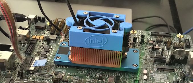 It has been hard to miss the fact that Intel has been vacuuming up a lot of industry talent, which brings with them a lot of experience. Renduchintala, Koduri, Keller, Hook, and Carvill, are just to name a few. This new crew has decided to break Intel out of its shell for the first time in a while, holding the first in a new tradition of Intel Architecture Days. Through the five hours of presentations, Intel lifted the lid on the CPU core roadmaps through 2021, the next generation of integrated graphics, the future of Intel’s graphics business, new chips built on 3D packaging technologies, and even parts of the microarchitecture for the 2019 consumer processors. In other words, it's many of the things we've been missing out on for years. And now that Intel is once again holding these kinds of disclosures, there’s a lot to dig in to. Contents ListIntel covered a good amount of ground at the Architecture Day, which we’ve split into the following categories:
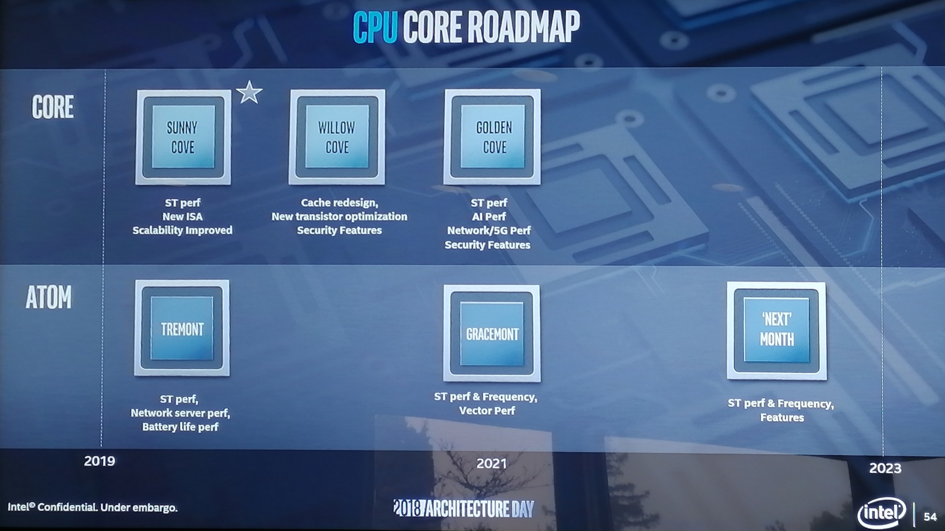
It is common for companies like Intel to ask members of the press what they enjoy about announcements from Intel, Intel’s competitors, or other companies in the industry. One of answers I will never tire of saying is ‘roadmaps’. The roadmap is a simple document but it enables a company to explain part of its future plans in a very easy to understand way. It shows to the press, to customers, and to partners, that the company has a vision beyond the next product and that it expects to deliver at a rough cadence, hopefully with some markers on expected performance additions or improvements. Roadmaps are rarely taken as set in stone either, with most people understanding that they have an element of fuzziness depending on external factors. To that end, I’ve been requesting Intel to show roadmaps for years. They used to be common place, but ever since Skylake, it has kind of dried up. In recent months Intel has shown rough datacentre roadmaps, with Cascade Lake, Cooper Lake, and Ice Lake and the next few generations. But for the Core family it has been somewhat more difficult. Depending on which analyst you talk to, a good number will point to some of the Skylake derivatives as being holding points while the issues with 10nm have been sorted out. But nonetheless, all we tend to hear about is the faint whisper of a codename potentially, which doesn’t mean much. So imagine my delight when we get not one roadmap from Intel on CPUs, but two. Intel gave us both the Core architecture roadmap and the Atom architecture roadmap for the next few generations.
For the high performance Core architecture, Intel lists three new codenames over the next three years. To be very clear here, these are the codenames for the individual core microarchitecture, not the chip, which is an important departure from how Intel has previously done things. Sunny Cove, built on 10nm, will come to market in 2019 and offer increased single-threaded performance, new instructions, and ‘improved scalability’. Intel went into more detail about the Sunny Cove microarchitecture, which is in the next part of this article. To avoid doubt, Sunny Cove will have AVX-512. We believe that these cores, when paired with Gen11 graphics, will be called Ice Lake. Willow Cove looks like it will be a 2020 core design, most likely also on 10nm. Intel lists the highlights here as a cache redesign (which might mean L1/L2 adjustments), new transistor optimizations (manufacturing based), and additional security features, likely referring to further enhancements from new classes of side-channel attacks. Golden Cove rounds out the trio, and is firmly in that 2021 segment in the graph. Process node here is a question mark, but we’re likely to see it on 10nm and or 7nm. Golden Cove is where Intel adds another slice of the serious pie onto its plate, with an increase in single threaded performance, a focus on AI performance, and potential networking and AI additions to the core design. Security features also look like they get a boost.
The lower-powered Atom microarchitecture roadmap is on a slower cadence than the Core microarchitecture, which is not surprising given its history. Seeing as how Atom has to fit into a range of devices, we’re expecting there to be a wide range in capabilities, especially from the SoC side. The upcoming microarchitecture for 2019 is called Tremont, which focuses on single threaded performance increases, battery life increases, and network server performance. Based on some of the designs later in this article, we think that this will be a 10nm design. Following Tremont will be Gracemont, which Intel lists as a 2021 product. As Atom is designed to continually push both the performance at the high-end of its capabilities and the efficiency at the low-end, Intel lists that Gracemont will have additional single threaded performance and a focus on increased frequency. This will be combined with additional vector performance, which likely means that Atom will get some wider vector units or support new vector instructions. Beyond this will be a future ‘mont’ core (and not month as listed in the image). Here Intel is spitballing what this new 2023 core might have, for which the general listing of performance, frequency and features is there.
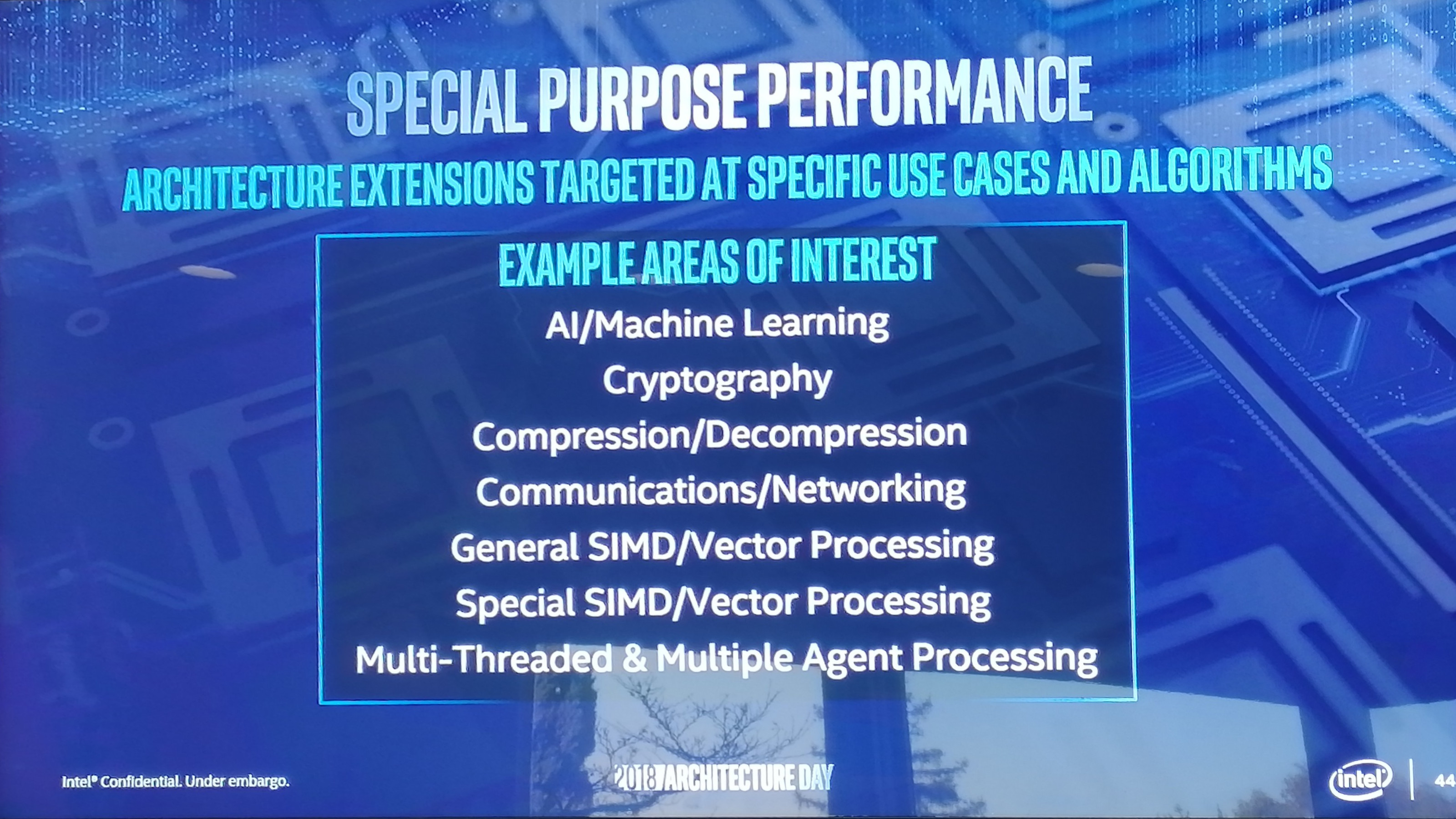
As stated above, these are just the microarchitecture names. The actual chips these cores are in will likely have different names, which means a Lake name for the Core microarchitecture. At the event, Intel stated that Ice Lake would have Sunny Cove cores in it, for example. Another aspect to Intel’s presentations was that future microarchitectures are likely to be uncoupled from any process technologies. In order to build some resiliency into the company’s product line moving forward, both Raja Koduri and Dr. Murthy Renduchintala explained that future microarchitectures will not be process dependent, and the latest products will come to market on the best process technologies available at the time. As a result we’re likely to see some of the Core designs straddle different manufacturing technologies. Intel also went into a bit of detail on microarchitecture of Sunny Cove. One of the best parts when a new microarchitecture is announced is learning how it all works and how it has changed. Intel has been on close variants of the Skylake core since Skylake first launched in 2015, which has carried through Kaby Lake, Coffee Lake, and Coffee Lake refresh – and so getting an update to his old core design is more than welcome. While I applaud Intel for getting something new to put in front of our faces, the level of information was unfortunately less than complete. For reasons of ‘we’ll discuss more nearer the launch’, Intel was only set on discussing the back end of the microarchitecture design in any detail. In core design parlance, this means everything beyond the dispatch and order queues. Intel framed its microarchitecture updates into two different sections: general purpose performance increases and special purpose performance increases. The company described the general purpose updates essentially as raw IPC (instructions per clock) throughput or an increase in frequency. An increase in either of these two leads to a performance increase no matter the code, at least as long as it is compute bound. Frequency is often a function of the implementation and process, whereas IPC increases can come from cores being wider (more executing instructions per clock), deeper (more parallelism per clock), and smarter (better data delivery through the front end).
The other type of performance increase is the special purpose kind, which means that certain workloads used in specific scenarios can be improved through additional acceleration methods, such as dedicated IP or specialized instructions.
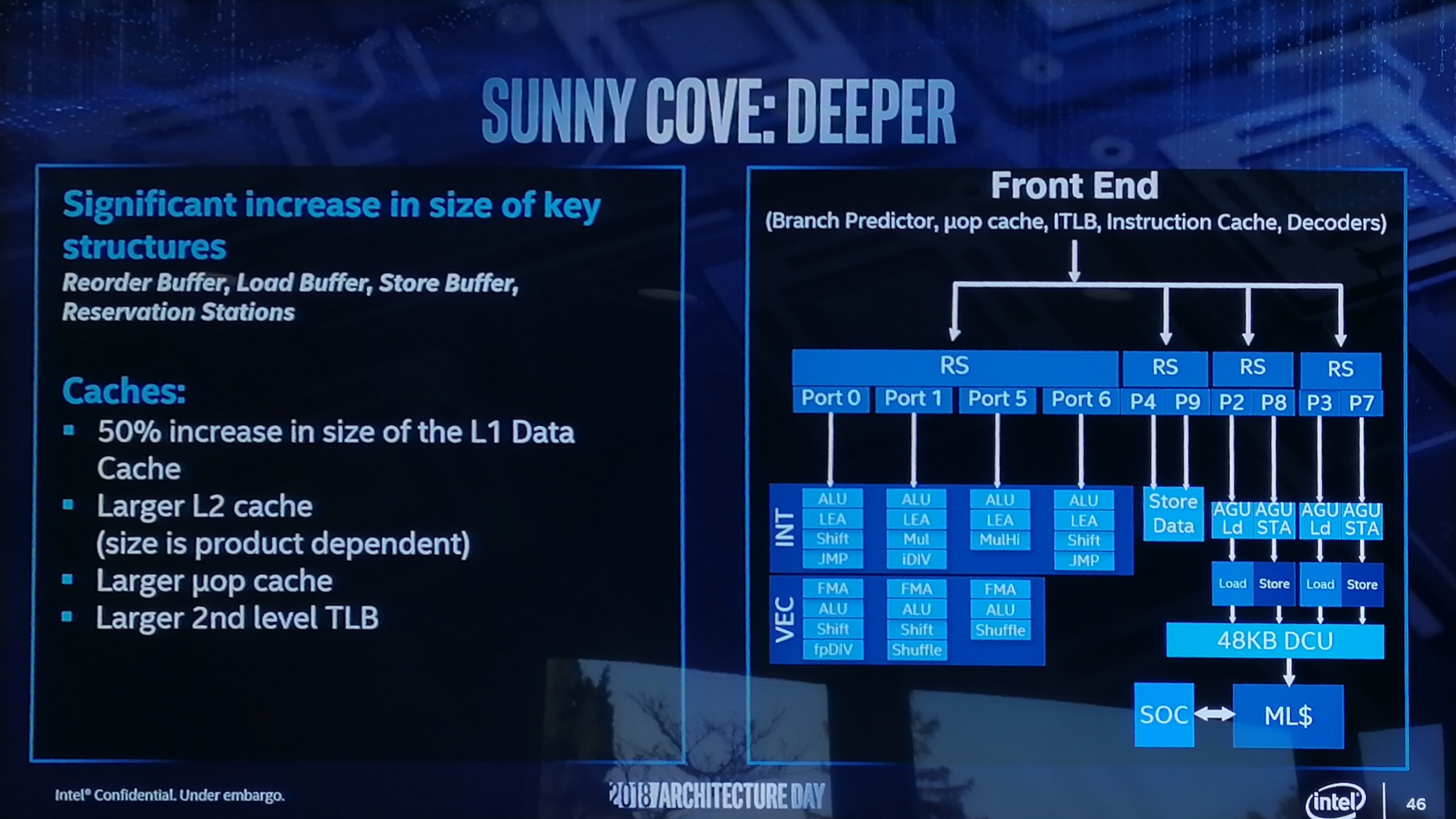
Sunny Cove is set to have both. On the back end of the microarchitecture design, Intel has done several things including increasing cache sizes, making the execution of the core wider, increasing L1 store bandwidth, and other things.
Starting with the cache improvements, the Sunny Cove core back end has a 48 KB L1 Data cache, upgraded from 32 KB. Normally cache misses decrease by a factor of a square root of the proportional size when the cache is increased, so in this case we should expect a 22% reduction in L1-Data cache misses. We are told that the L2 cache size has also been increased in both the Core and Xeon variants of Sunny Cove (256 KB and 1 MB respectively), although to exactly what size will be revealed at a later date. While not back-end, the micro-op (uOp) cache has increased from a 2048-entry design, although exactly to what Intel is not saying at this point. The second level TLB size has also increased, which will help with machine address translation of recent addresses – normally this is increased when more lookups need to be kept and stored, which means that Intel identified a number of use cases where recent addresses had been evicted shortly before being needed.
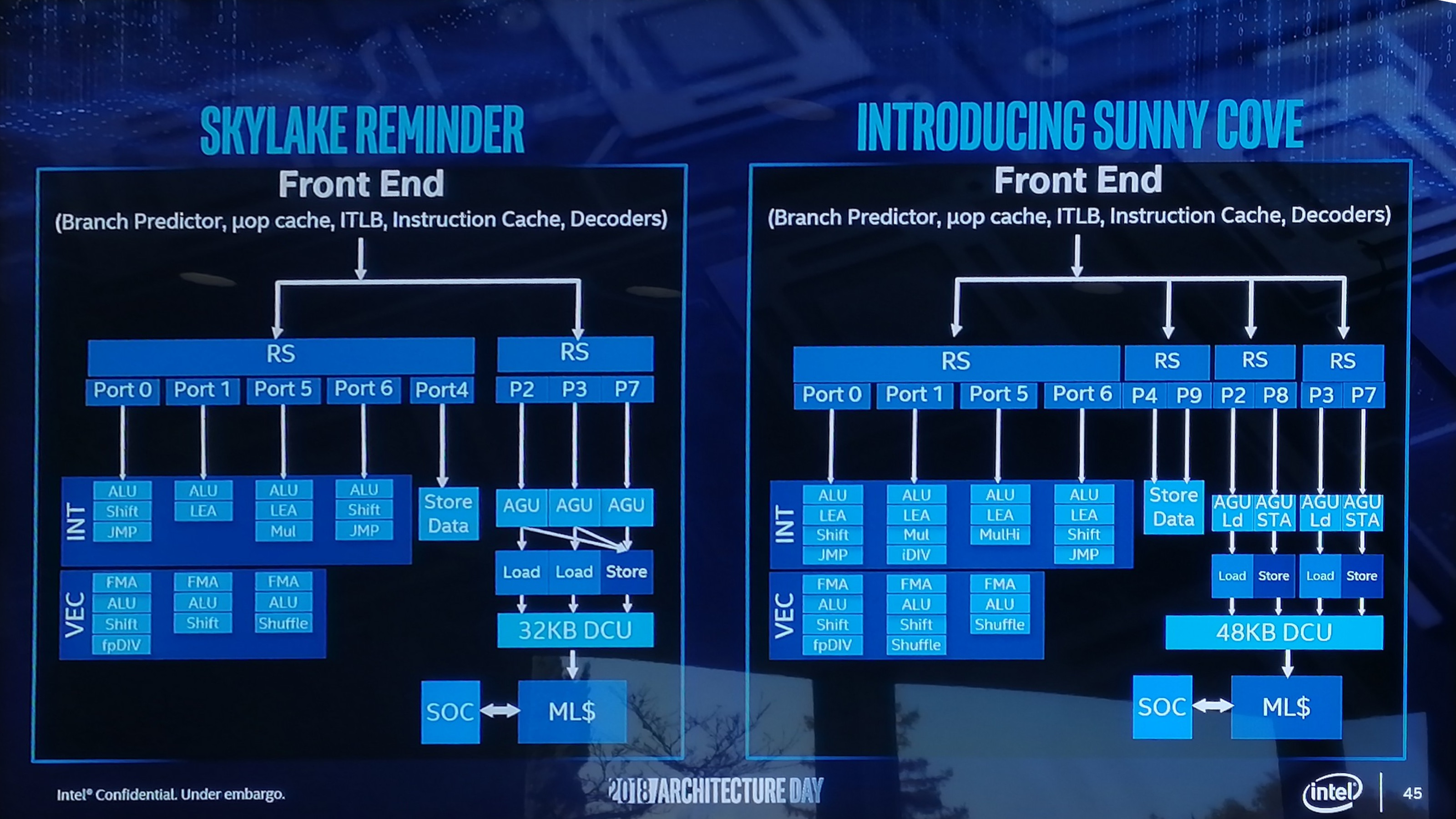
From the diagram we can see some other changes, such as the increase in execution ports from eight to ten, allowing more instructions to come out of the schedulers at one time. Port 4 and Port 9 is linked to a cycling data store, doubling that bandwidth, but also the AGU store capabilities have doubled, for which the increased L1-D size will help. Previously on Skylake there was a potential bottleneck when all three AGUs could attempt a store, however only enough bandwidth was present for one per clock cycle. Load performance is unaffected. There is also an allocation increase, moving from four to five. This means that the dispatch out of the reorder buffer can now hit five instructions per cycle, rather than four – however given that the ops/cycle out of the Skylake decoders and uOp cache was four-to-five (depending on certain factors), it will be interesting to see how the front end has changed as a result. There are also substantial changes in the execution ports between Skylake and Sunny Cove, which is best represented in a diagram and a table:
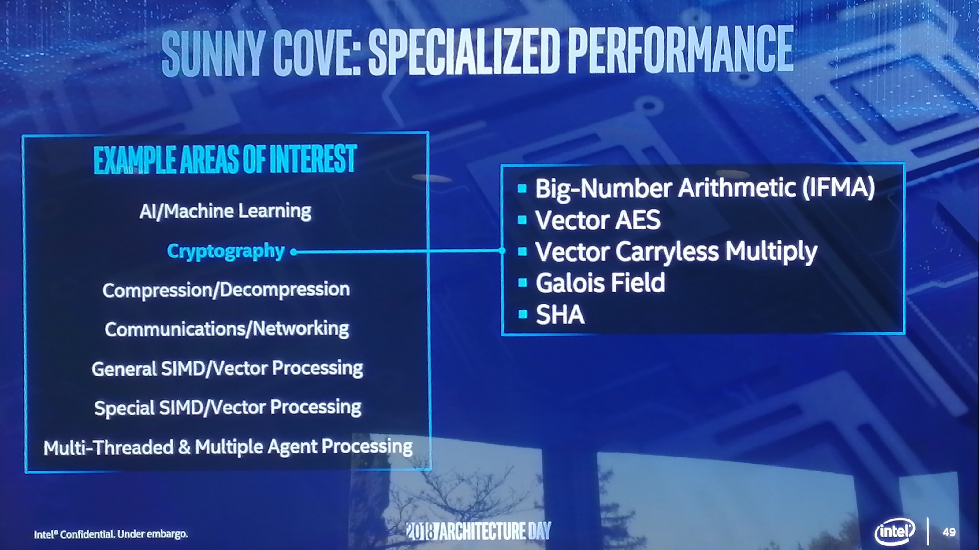
The parts highlighted in bold are different in the Sunny Cove core. We see that Intel has equipped the Integer section of the core with more LEA units to help with memory addressing calculations, possibly to help improve performance loss with security mitigations that require frequent memory calculations or to help with high-performance array code with constant offsets. Port 1 gets the Mul unit from Skylake Port 5, probably for rebalancing purposes, but there is also an integer divider unit here. This addition is a bit of a tweak, as we know that Cannon Lake has a 64-bit IDIV unit in its design as well. In that case it brings 64-bit integer division down from 97 clocks (a mix of instructions) down to 18 clocks, and this is likely something similar. Also on the INT side is that Port 5’s multiply unit has become a ‘MulHi’ unit which in other implementations leave most-significant nibble of the result in a register for further use. I'm not sure exactly what its position is here in the Sunny Cove core though. On the FP side, Intel has increased the shuffle resources, which we are told was because they had customers requesting this functionality to help remove bottlenecks in their code. Intel didn’t state the capabilities for the FMAs in the FP part of the core, however we do know that the core has an AVX-512 unit, so at least one of these FMAs should interface with it. Cannon Lake only has one 512-bit FMA, and that most likely carries over here, and the Xeon Scalable version might get two. I would like to get proved wrong though. Other updates to the core as listed from Intel include improvements to the branch predictor and a reduced ‘effective load latency’ (due to the TLB and L1-D), although it was pointed out that these improvements won’t help everyone, and might require new algorithms in order to use specific parts of the core. We’re waiting to see what changes Intel has made on the front-end, which is where a lot of low-hanging fruit often lies for performance. On top of the microarchitecture differences, there are new instructions for the Sunny Cove core to help speed up specialist compute tasks. With the AVX-512 unit in play, the new core will support IFMA instructions for big arithmetic compute, and which are also useful in cryptography. Along the same lines, Vector-AES (supporting more AES concurrently) and Vector Carryless Multiply are also supported. SHA and SHA-NI instructrions are also added, along with Galois Field instructions, which are fundamental building blocks in some elements of cryptography as well.
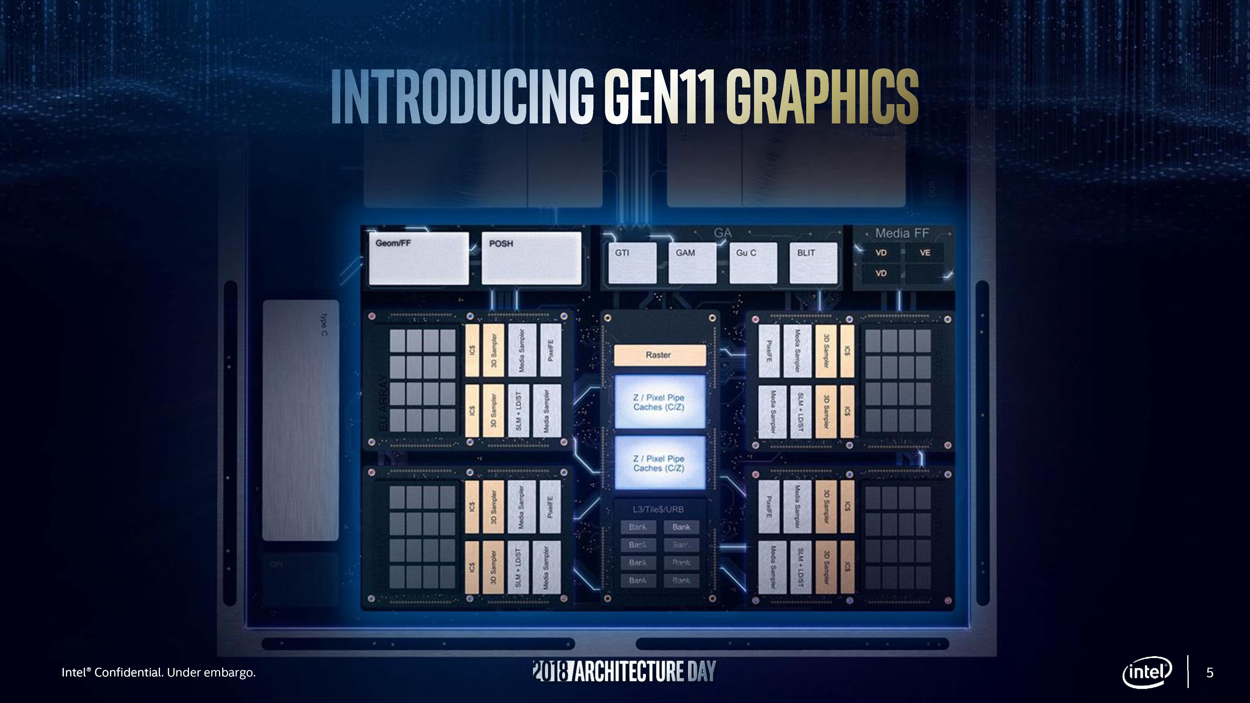
For Sunny Cove, there is also built-in support for larger memory capacities. The paging table for main memory is now a five layer design, up from four layers, supporting a Linear Address space up to 57 bits and a physical address space up to 52 bits. This means, according to Intel, that the server processors could theoretically support 4 TB of memory per socket. We will see Sunny Cove hit the market in the server space with Ice Lake-SP in 2020 according to Intel’s previous Xeon roadmaps. For security, Sunny Cove has access to Multi-Key Total Memory Encryption, and User Mode Instruction Prevention. So where does this leave us in terms of Sunny Cove predicted performance compared to Skylake at a clock for clock level? Unfortunately we don’t have enough information. There is only enough to whet the appetite. Intel wants you (and me) to come back for more in 2019. Some of the first words out of the mouth of Raja Koduri about graphics is that Intel has a duty to its one billion customers with integrated graphics to give them something that is useful, and that it is time for Intel to provide graphics which people can actually play games on. Given his expertise on the matter, it shouldn’t sound too far-fetched: more people play games than ever before, and these users want to play no matter what their hardware. To that end, Raja stated that Gen11 graphics is the first step in a new graphics policy to provide the performance and features to let gamers play the most popular games, no matter what implementation. Gen11: Intel’s first GT2 TFLOPS GraphicsIn 2015, Intel launched the Skylake processor with Gen9 integrated graphics. Rather than moving straight to Gen10 the next time around, we were given Gen 9.5 in both Kaby Lake and Coffee Lake, which supposedly draw features from what would have been Gen 10. Actually, the graphics for Intel’s failed 10nm Cannon Lake chip were meant to be called Gen10, however Intel never released a Cannon Lake processor with working integrated graphics, and because Gen11 goes above and beyond what Gen10 would have been, we’ve gone straight to Gen11. Make sense? Well Intel didn’t even bother to acknowledge Gen10 in its history graph:
We will see Gen11 graphics being paired with Sunny Cove cores on 10nm sometime in 2019 according to the roadmaps. However rather than give a detailed architecture layout for the new product, we instead were given a rather high level diagram.
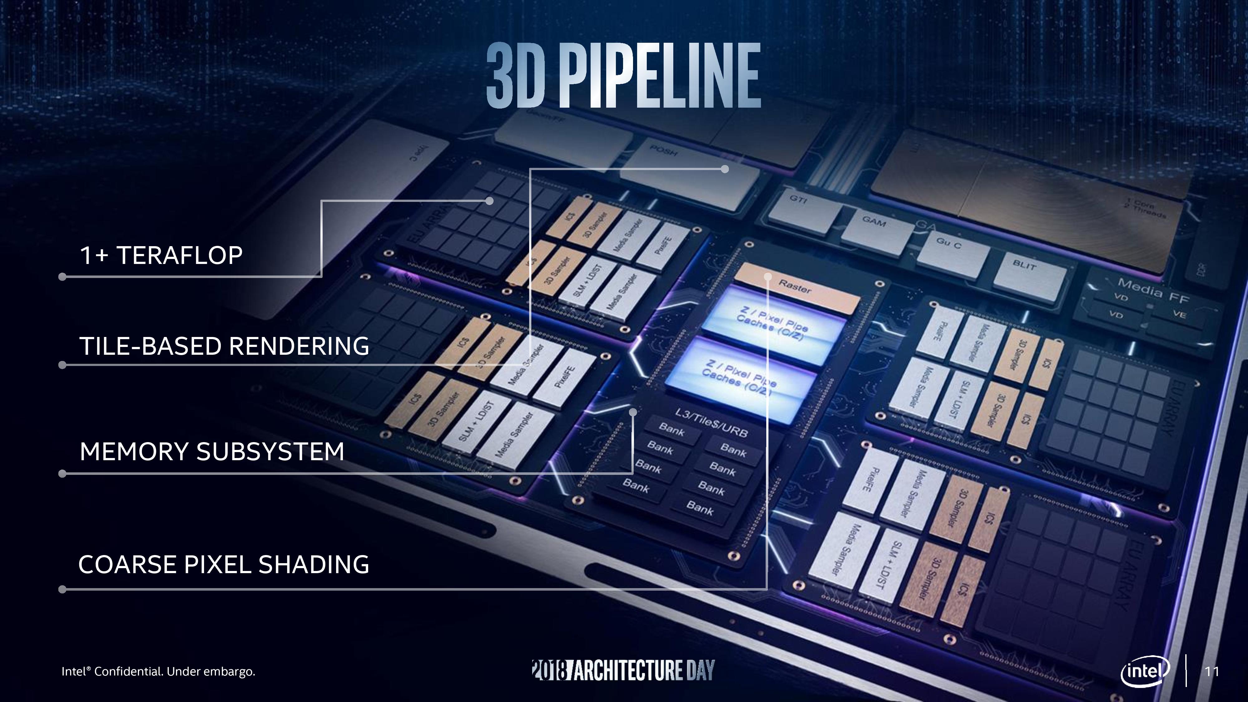
From here we can deduce a few things. We were told that this configuration is the GT2 config, which will have 64 execution units, up from 24 in Gen9.5. These 64 EUs are split into four slices, with each slice being made of two sub-slices of 8 EUs a piece. Each sub-slice will have an instruction cache and a 3D sampler, while the bigger slice gets two media samplers, a PixelFE, and additional load/store hardware. Intel lists Gen11 targeting efficiency, performance, advanced 3D and media capabilities, and a better gaming experience. Intel didn’t go into too much detail regarding how the EUs are at higher performance, however the company did say that the FPU interfaces inside the EU are redesigned and it still has support for fast (2x) FP16 performance as seen in Gen9.5. Each EU will support seven threads as before, which means that the entire GT2 design will essentially have 512 concurrent pipelines. In order to help feed these pipes, Intel states that it has redesigned the memory interface, as well as increasing the L3 cache of the GPU to 3 MB, a 4x increase over Gen9.5, and it is now a separate block in the unslice section of the GPU.
Other features include tile-based rendering, which Intel stated the graphics hardware will be able to enable/disable on a render pass basis. This will make Intel the final member of the PC GPU vendor community to implement this, following NVIDIA in 2014 and AMD in 2017. While not a panacea to all performance woes, a good tile rendering setup plays well to the bandwidth limitations of an integrated GPU. Meanwhile Intel's lossless memory compression has also improved, with Intel listing a best case performance boost of 10% or a geometric mean boost of 4%. The GTI interface now supports 64 bytes per clock read and write to increase throughput, which works with the better memory interface. Coarse Pixel Shading, Intel's implementation of multi-rate shading and similar in scope to NVIDIA’s own Variable Pixel Shading, is also supported. This allows the GPU to reduce the amount of total shading work required by shading some pixels on a less than 1:1 basis. Intel showed two demos for CPS, where pixel shading was reduced either as a function of object distance from camera (so you do less work when things are further away), or reduced as a function of how close the object is to the center of the screen, designed to help features like foveated rendering for VR. With a 2x2 pixel stencil applied – meaning only one pixel shading operation was done per block of 4 pixels – Intel stated a ~30% increase in frame rates in supported games. Unfortunately this needs to be applied on a game-by-game basis in order to prevent significant image quality losses, so the performance gains won't be immediate or universal.
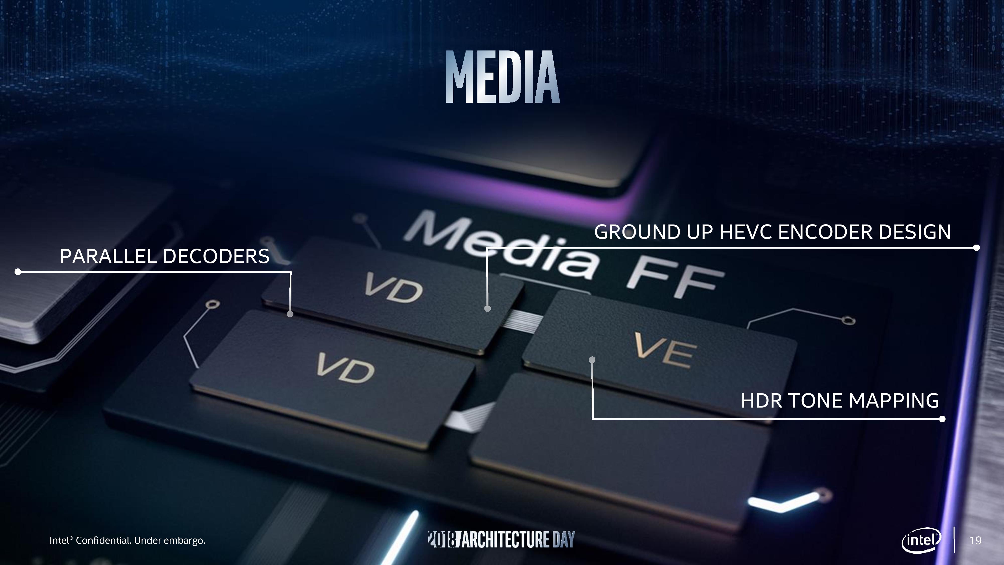
For the media block, Intel says that the Gen11 design includes a ground up HEVC encoder design, with high quality encode and decode support. Intel cited the fact that its media fixed function units are already used in the datacenter for video processing, and home users can take advantage of the same hardware. Intel also stated that by using parallel decoders it can either support concurrent video streams or they can be combined to support a single large stream, and this scalable design will allow future hardware to push the peak resolutions up to 8K and beyond.
The highlight of the display engine is support for Adaptive Sync technologies. We were told that it was announced back at the launch of Skylake, but now it is finally ready to go into Intel’s integrated graphics. This goes in hand with HDR support due to its high-precision data path.
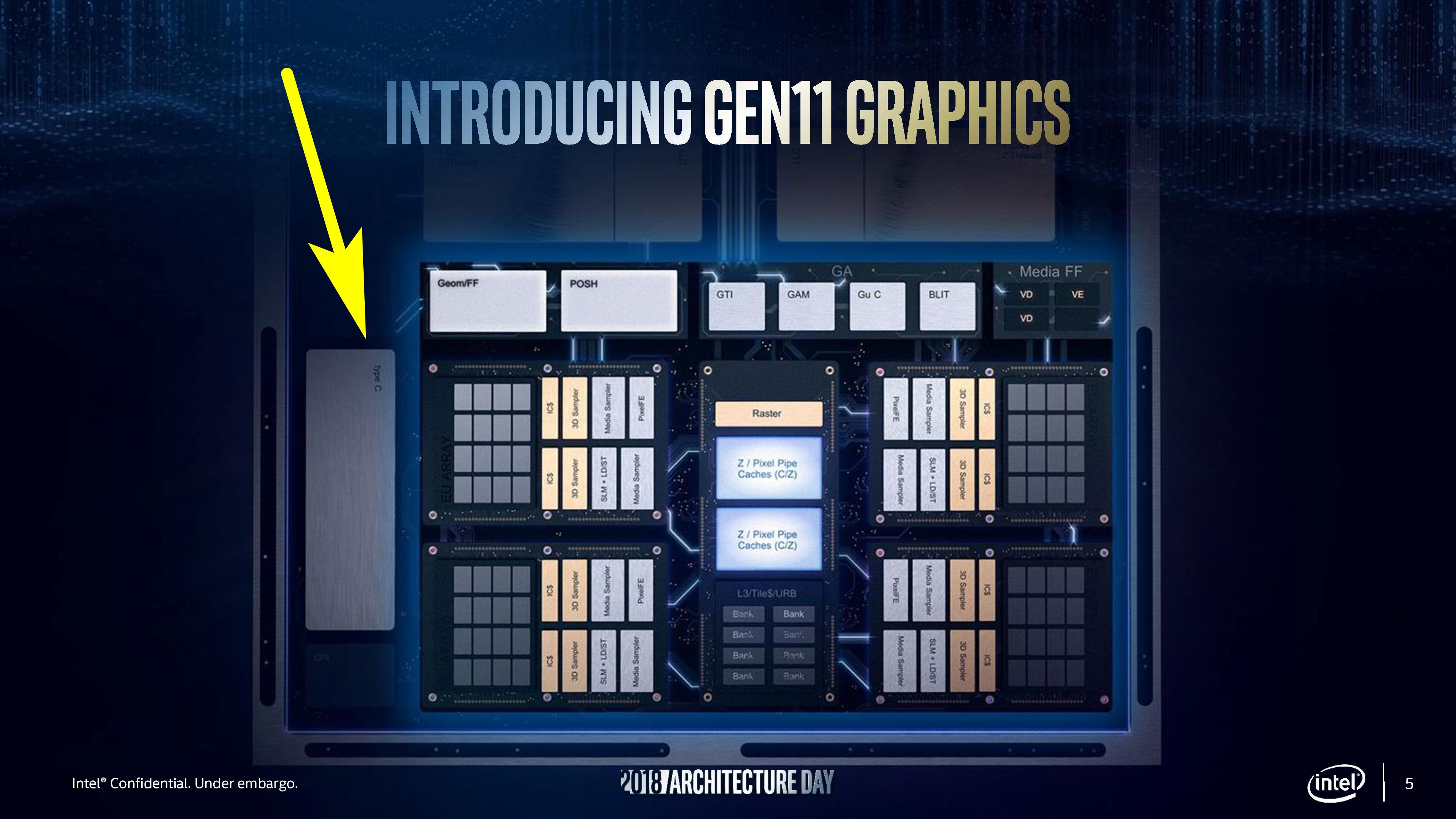
One thing in this presentation that Intel didn’t mention directly is that Gen11 graphics would appear to have Type-C video output support, potentially indicating that Intel has integrated the necessary mux into the chipset itself, removing another IC from the motherboard design. As part of the Architecture Event, Intel ran a number of demos on a chip that was supposedly based on the new Sunny Cove cores and Gen11 graphics.
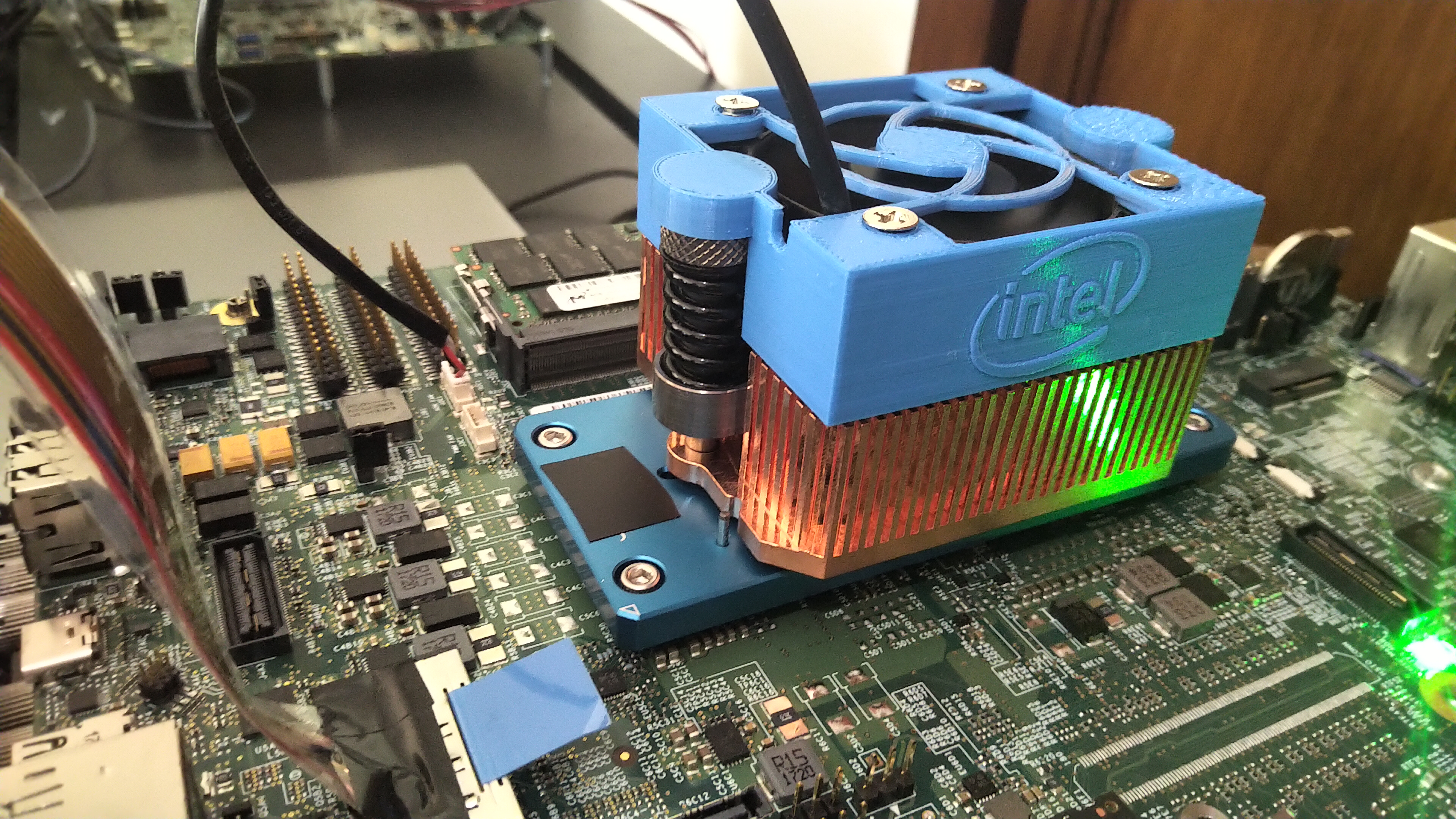
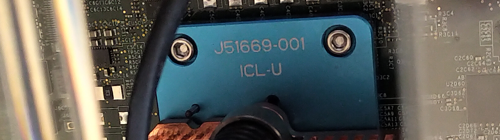
These were development systems with these funky looking heatsinks and loud fans to ensure there was no thermal throttling. One thing worth noticing is that black bit of tape on the heatsink here, which wasn’t present on one of the other demo units.
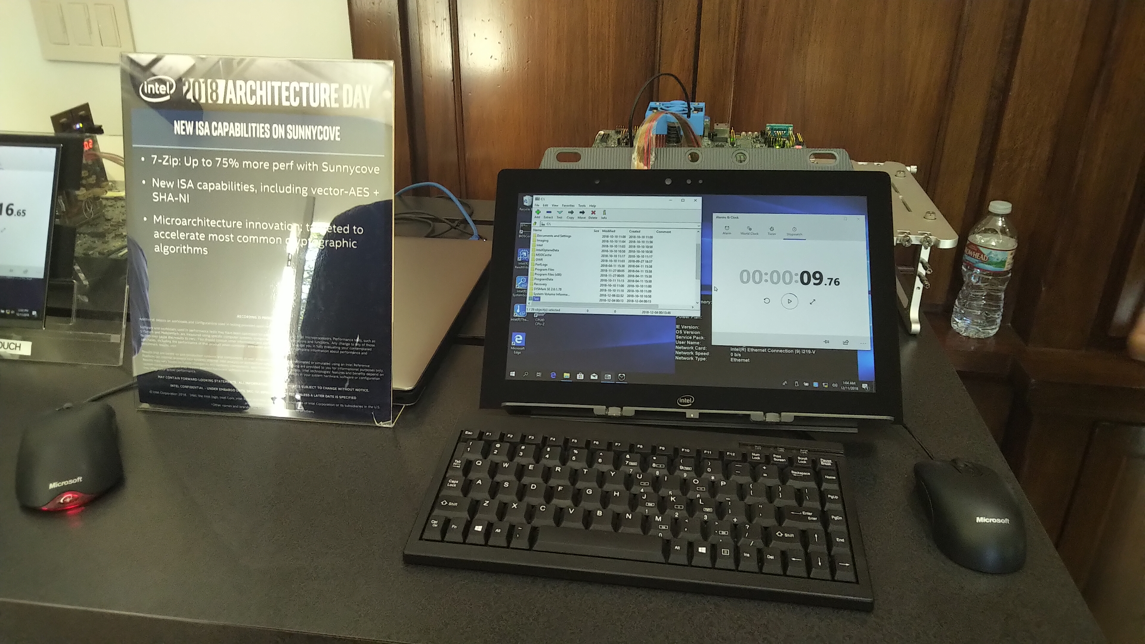
Hello Ice Lake-U. Being a U-series heatsink, this means that the Core is likely designed for a 15W scenario. Perhaps it’s no surprise that Intel wasn’t giving anything away in terms of the exact core count on display, speeds, feeds, and power. The demos that were present involved 7-Zip and gaming.
The 7-Zip demo was relatively straight forward, showing how the new instructions such as Vector-AES and SHA-NI in Sunny Cove can give the processor a 75% boost in performance over an equivalent Skylake based platform at iso-frequency. This falls under the ‘specialist’ improvements to the core rather than the general purpose improvements.
The other demo was Tekken 7, being run on a Sunny Cove + Gen11 machine and compared to a Skylake + Gen9 implementation. It looked a good deal smoother that’s for sure, however it was clear that it had some way to go to be fully out of the 30 FPS minimums. Not content with merely talking about what 2019 will bring, we were given a glimpse into how Intel is going to approach its graphics business in 2020 as well. It was at this point that Raja announced the new product branding for Intel’s discrete graphics business:
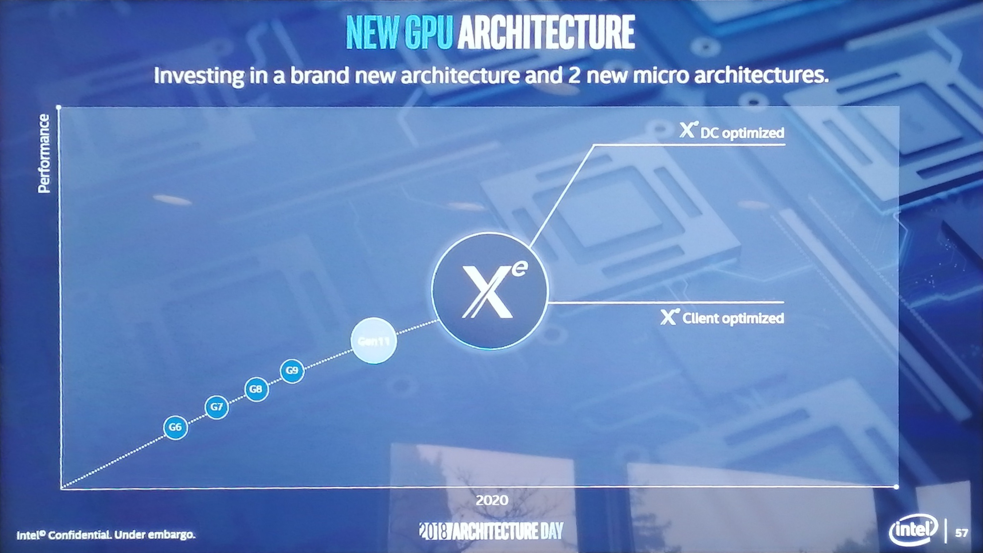
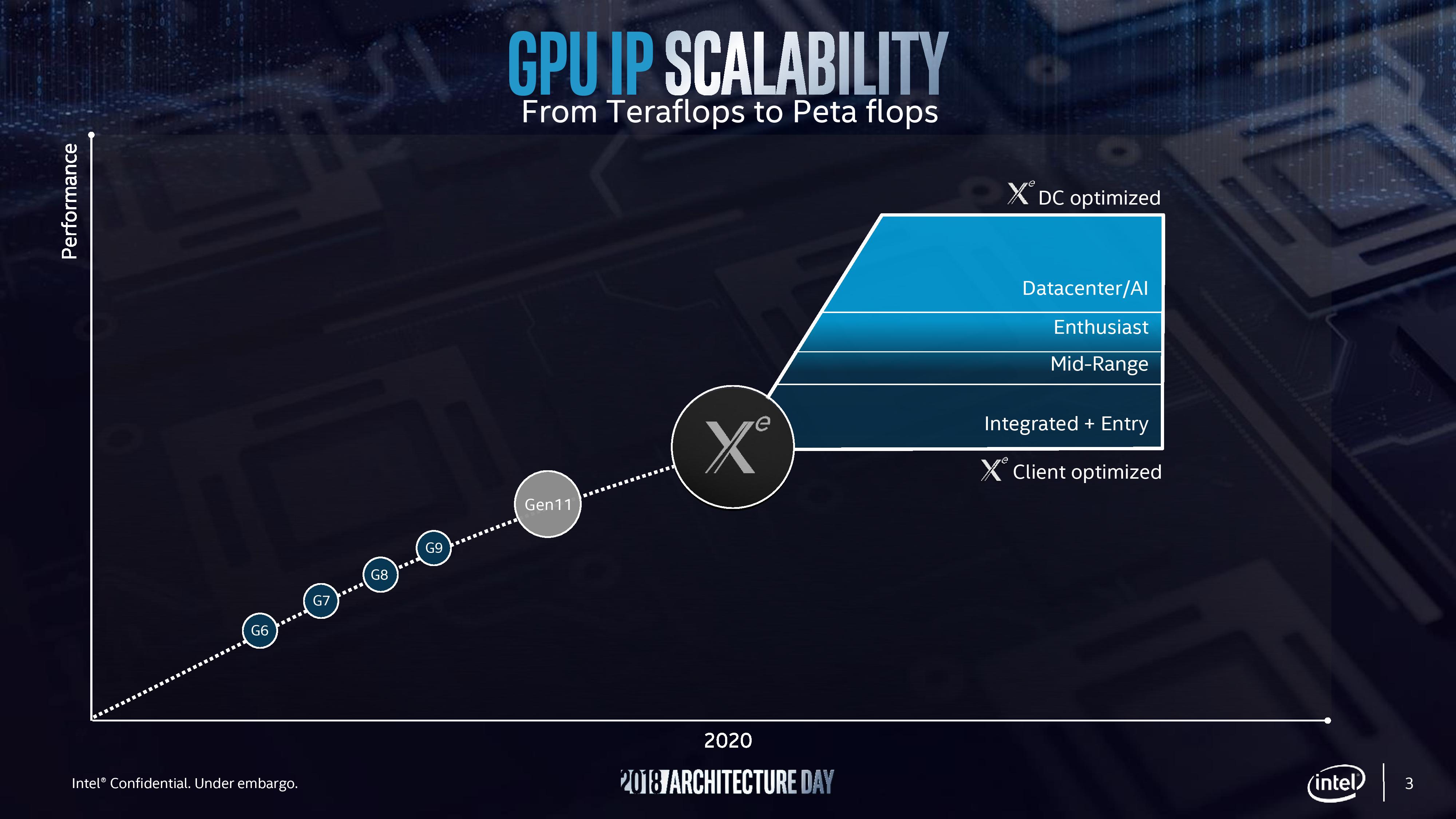
Intel will use the Xe branding for its range of graphics that were unofficially called ‘Gen12’ in previous discussions. Xe will start from 2020 onwards, and cover the range from client graphics all the way to datacenter graphics solutions.
Intel actually divides this market up, showing that Xe also covers the future integrated graphics solutions as well. If this slide is anything to go by, it would appear that Intel wants Xe to go from entry to mid-range to enthusiast and up to AI, competing with the best the competition has to offer. Intel stated that Xe will start on Intel’s 10nm technology and that it will fall under Intel’s single stack software philosophy, such that Intel wants software developers to be able to take advantage of CPU, GPU, FPGA, and AI, all with one set of APIs. This Xe design will feed the foundation of several generations of graphics, and shows that Intel is now ready to rally around a brand name moving forward. There was some confusion with one of the slides, as it would appear that Intel might be using the new brand name to also refer to some of it's FPGA and AI solutions. We're going to see if we can get an answer on that in due course. Anyone who has followed any amount of chip design in semiconductors should well-aware that most of the CPUs and SoCs in production today are based on monolithic dies – single pieces of silicon the have all what is needed inside, before being placed on a package and into a system. While rarer, there are multi-chip packages, were multiple chips go in one package with a shared connection. Beyond this we have seen interposers or embedded bridges designed to bring different chips together with high-speed interconnects. Now Intel is ready to bring 3D stacking into the mass market. One of the biggest challenges in modern chip design is minimizing die area. A small die decreases costs – typically power too – and can make it easier to implement in a system. When it comes down to extracting performance however, we are at the limits of scale – one of the downsides of big monolithic dies, or even multi-chip packages, is that memory is too far away. Intel today is now ready to talk about its Foveros technology, which involves active interposers in small form factors to bring differentiated technologies together. Foveros: It’s Greek for Awesome, ApparentlyThe way Raja introduced this technology started with discussing process technologies. Intel has for many years/decades been focused on high performance process nodes, trying to extract as much as possible from its high-performance cores. Alongside this, Intel also runs an IO optimized process node on a similar cadence but more suitable for PCH or SoC-type functions.
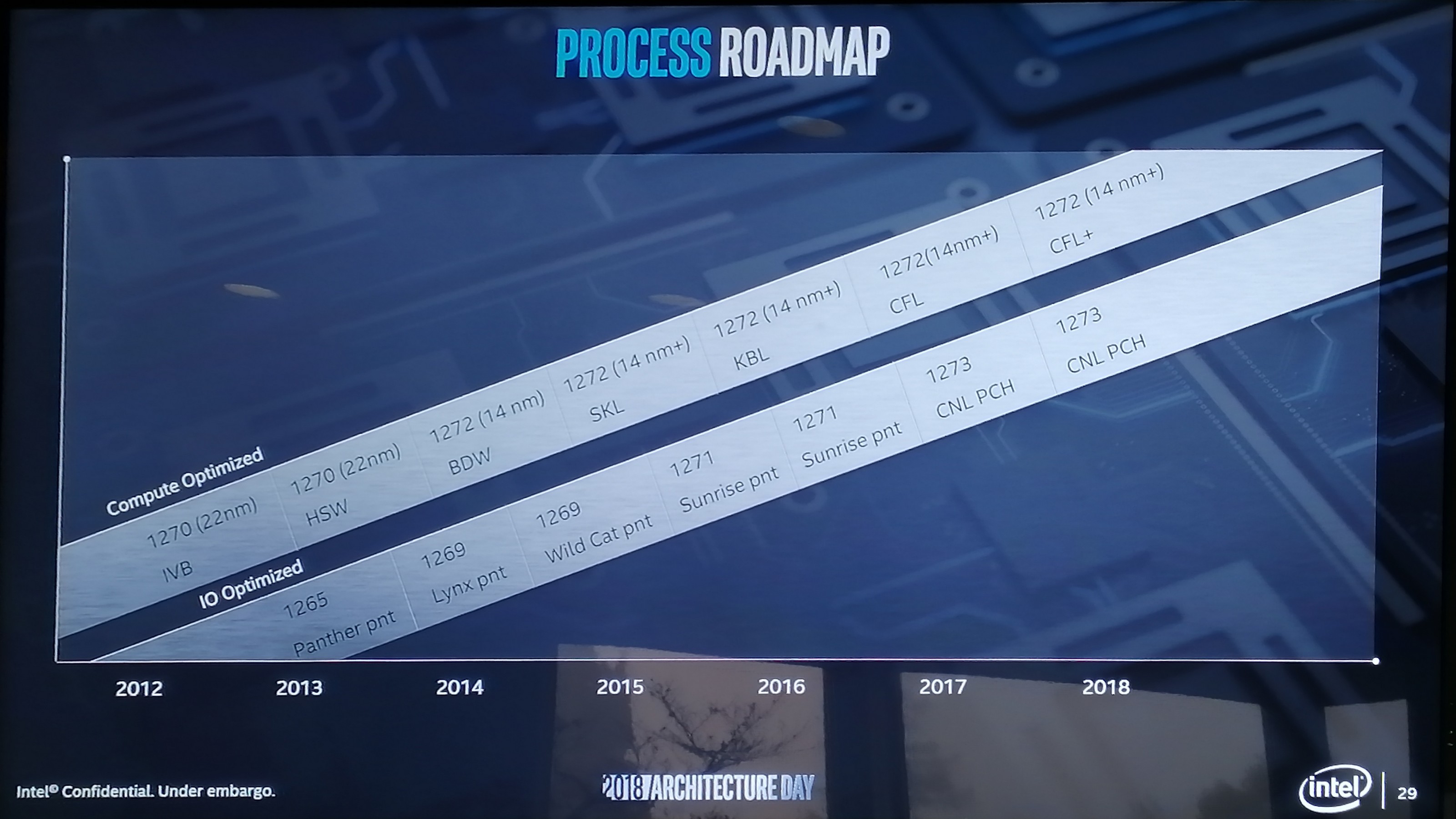
The 126x and 127x are the internal numbering systems for Intel’s process node technologies, although they don’t differentiate between BKM updates for the "+" node variants it turns out. But the point here is that Intel already knows that it needs certain process optimizations in place depending on the type of transistors, performance, and power needed. Going forward, Intel is going to be expanding its node base out so it can cover more power and performance points.
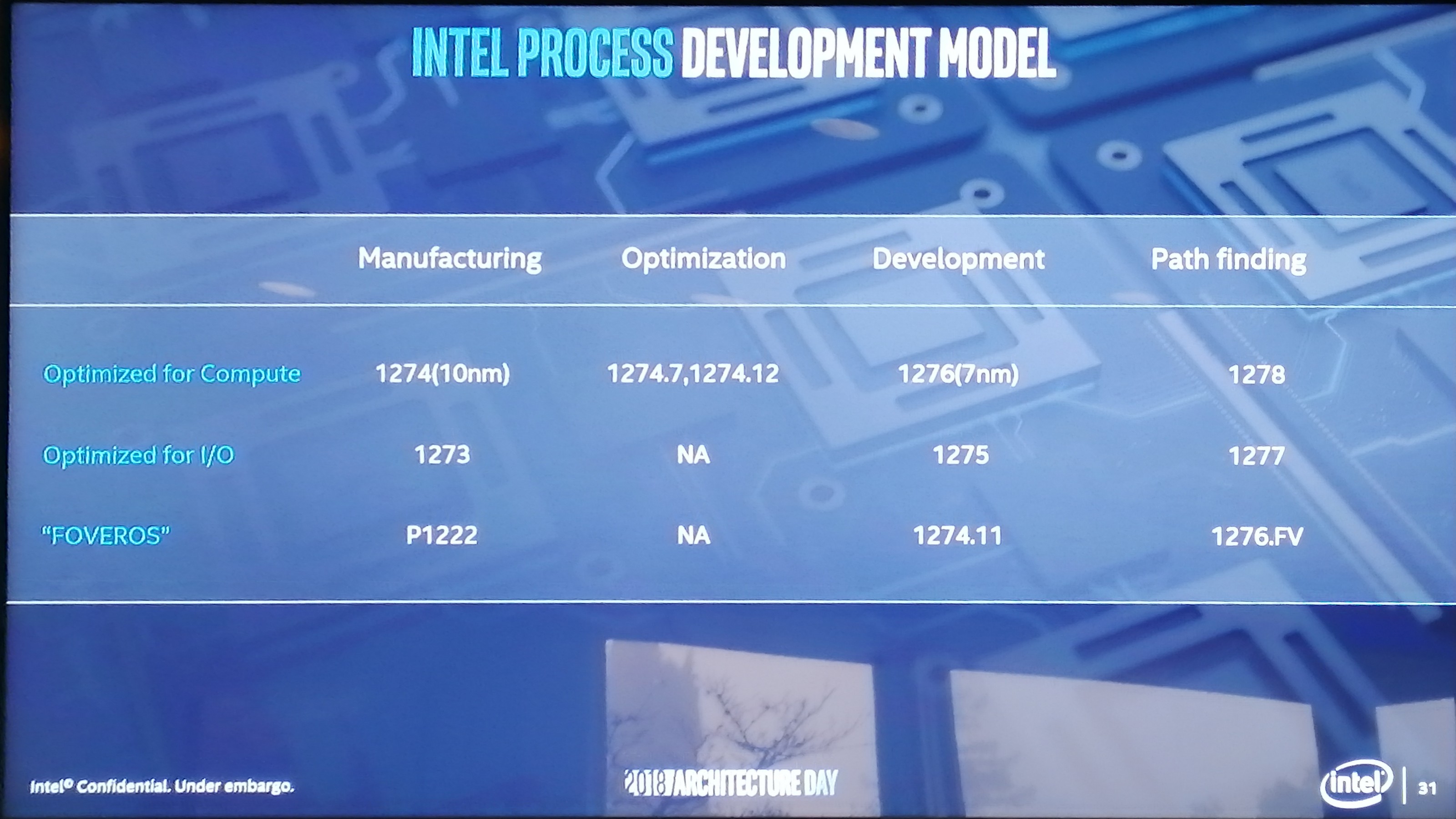
So for this example, Raja pulled out the current set of process technologies for 2019. For a manufacturing process, compute has the 1274 process on 10nm, IO has the 1273 process (14nm), while this new special Foveros technology is under P1222. Alongside the manufacturing, Intel will be working on optimizations focusing on the compute aspects of the manufacturing node. There will also be a set of developments for future node technologies, and the final column shows that Intel has path-finding research to look into future technologies and determine what capabilities will be possible on future designs. This sounds pretty much what a company like Intel should be doing, so no argument from me so far. The goal here is that each type of transistor use case can be different, and there isn’t a one-size fits all approach.
One way to assist with this is through chiplets and packaging. By picking the best transistor for the job in each case, whether it is CPU, GPU, IO, FPGA, RF, or anything else, with the correct packaging, it can be put together to get the best optimizations available.
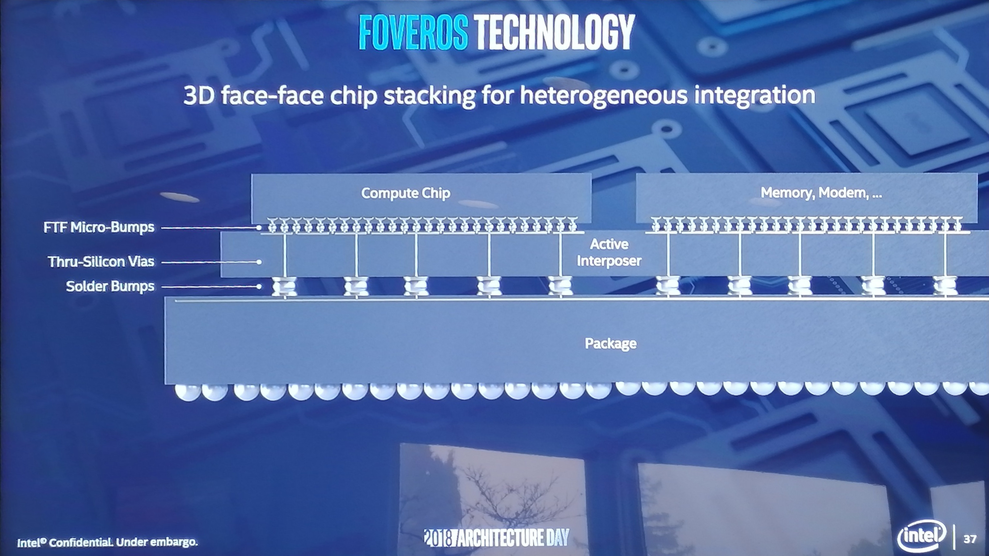
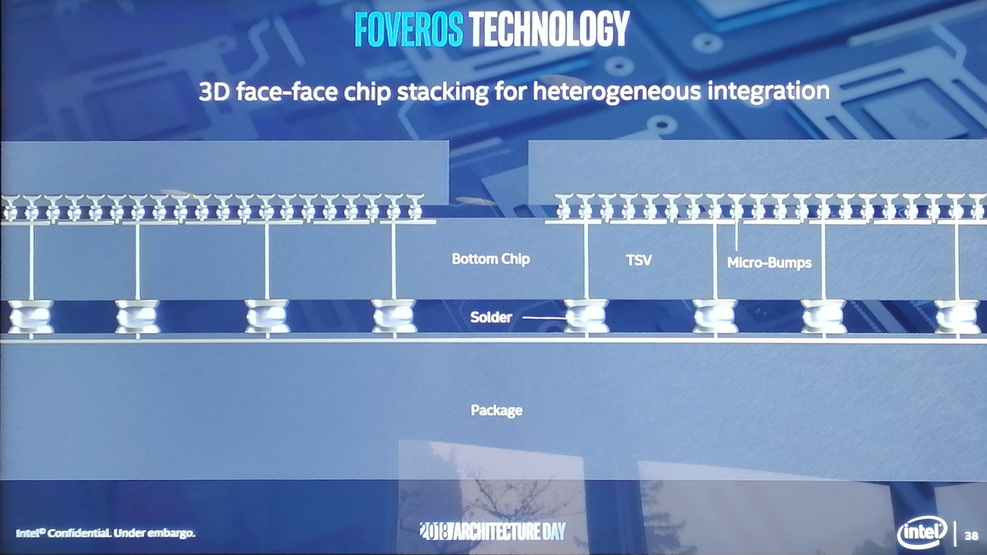
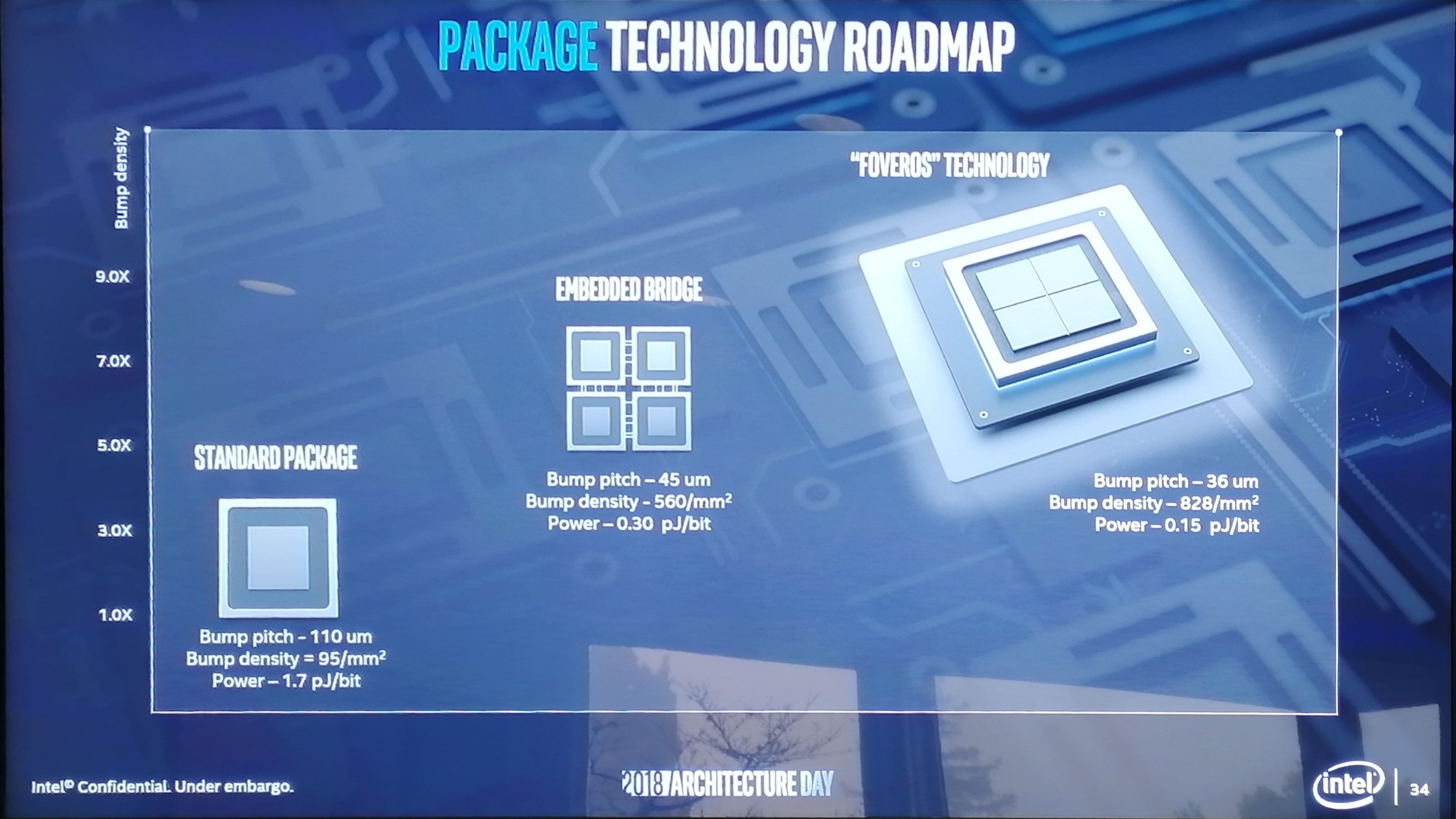
So here’s where Foveros fits in. Foveros is Intel’s new active interposer technology designed as a step above its own EMIB designs for small form-factor implementations, or those with extreme memory bandwidth requirements. For these designs the power per bit of data transferred is super low, however the packaging technology has to deal with the decreased bump pitch, the increased bump density, and also the chip stacking technology. Intel says that Foveros is ready for prime time, and they can produce it at scale.
So this Foveros ‘3D’ packaging just sounds like a silicon interposer, such as what we’ve seen on AMD’s Fiji or NVIDIA’s high-end datacenter GPUs. However Intel is going above what those products are doing by actually making the interposer part of the design. The interposer contains the through-silicon vias and traces required to bring power and data to the chips on top, but the interposer also carries the PCH or IO of the platform. It is, in effect, a fully working PCH, but with vias to allow chips to be connected on top.
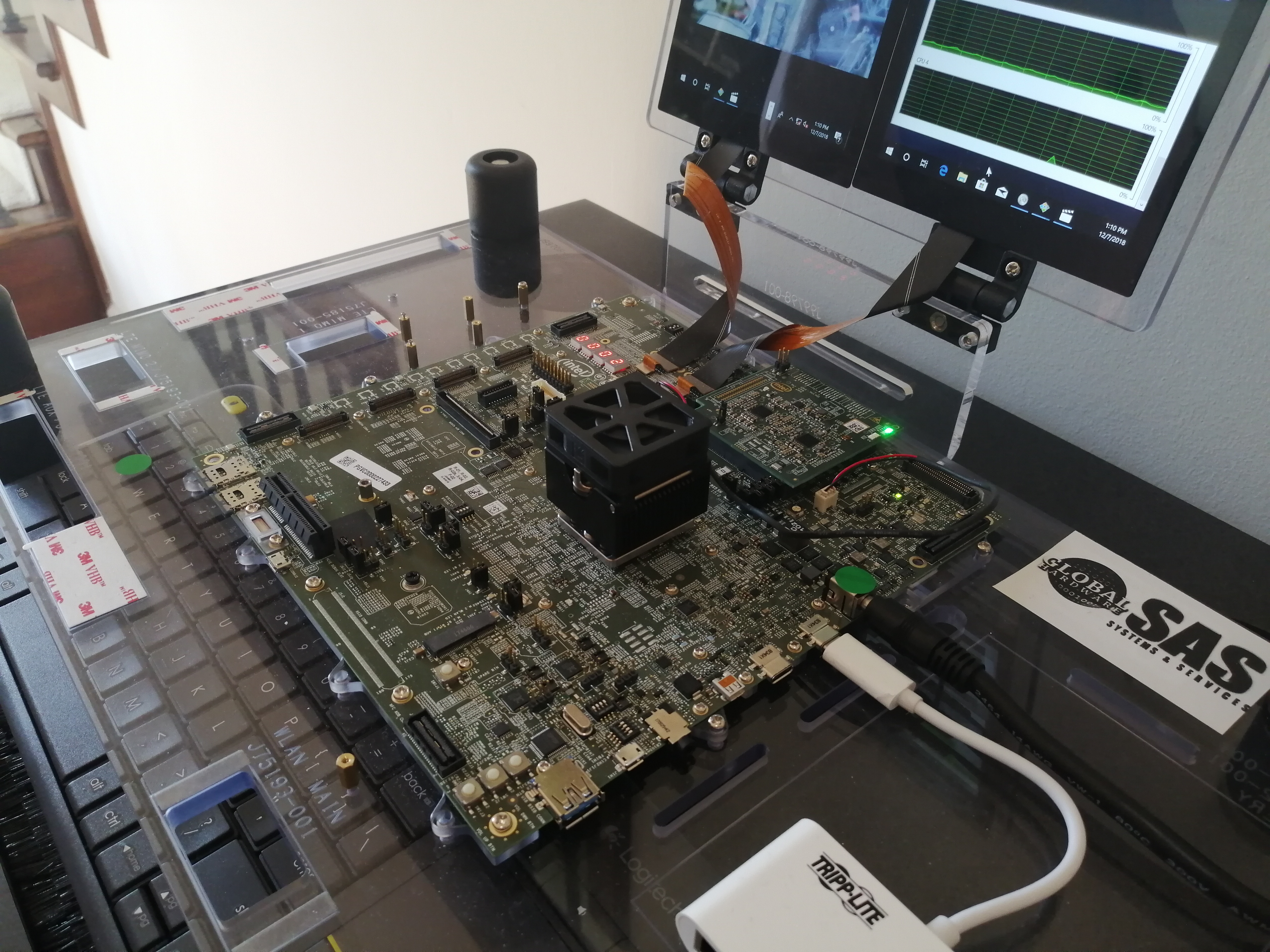
The first iteration of this technology is less complicated that the slide above, just using a set of CPU cores attached to the PCH below, but the idea is that a large interposer can have select functions on it and those can be removed from the chips above to save space. This also lets Intel use the different transistor types in different chips – the example we were given uses an interposer built on the 22FFL process node, with a 10nm set of CPUs on the top die. Above this, DRAM is provided in a POP package. Sounds cool, right? In actual fact, Intel had a Foveros chip or two working in the demo area. These, Intel explained, were hybrid x86 designs that combined a single big Core with four smaller Atom cores on the same 10nm piece of silicon. I’m sure I’ve heard about big.Little before, but I was shocked that Intel is actually going to do it! We managed to take a photo of the block diagram, which Intel removed from its slide deck before sending it out to the press after the presentations. All details on the next page. Perhaps someone will correct me, but I can’t ever remember a time when Intel has put multiple x86 cores of different configurations on the same bit of silicon (ed: Intel Edison). Ever since Arm starting doing it with its big.Little designs in smartphones, a perennial question was if Intel was going to do something similar, either with big and small Atom cores, or by moving a high-performance Core into the mix. When Intel left the smartphone and tablet market, we assumed the idea was dead. But, like a reanimated zombie, it has risen from the grave. Enter Intel’s Hybrid x86 CPU.
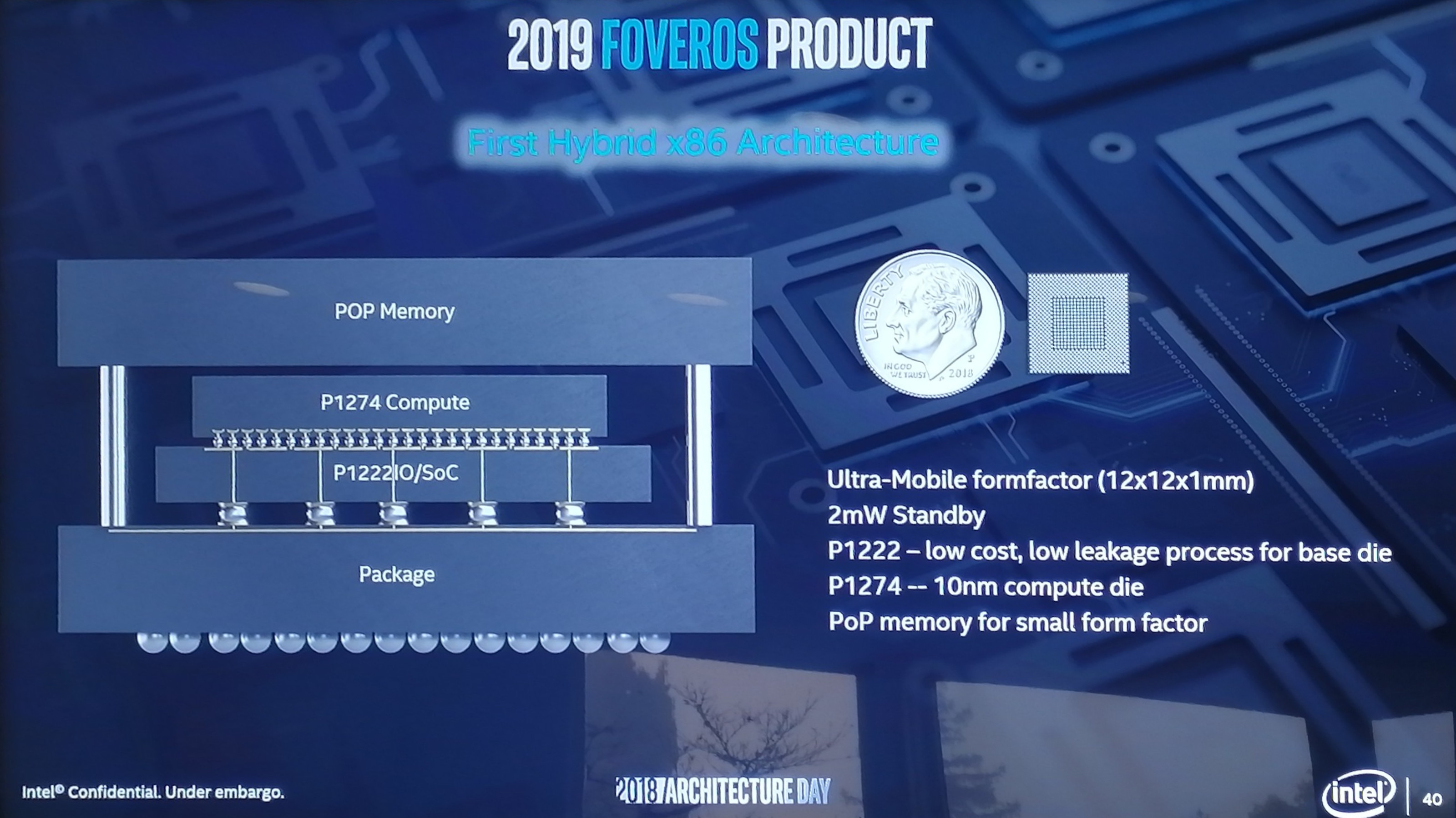
This tiny 12x12 package is built using Intel’s Fovoros technology, using a 22FFL IO chip as the active interposer connected with TSVs to a 10nm die that contains both a single Sunny Cove core and four Atom (Tremont?) cores. This tiny chip is smaller than a dime, and is designed to have a 2 mW standby power. It would appear that this chip is destined for mobile devices.
Here’s the manufacturing diagram, showing the idea that POP memory is placed over the Fovoros design to give the final product. Very much like a mobile chip.
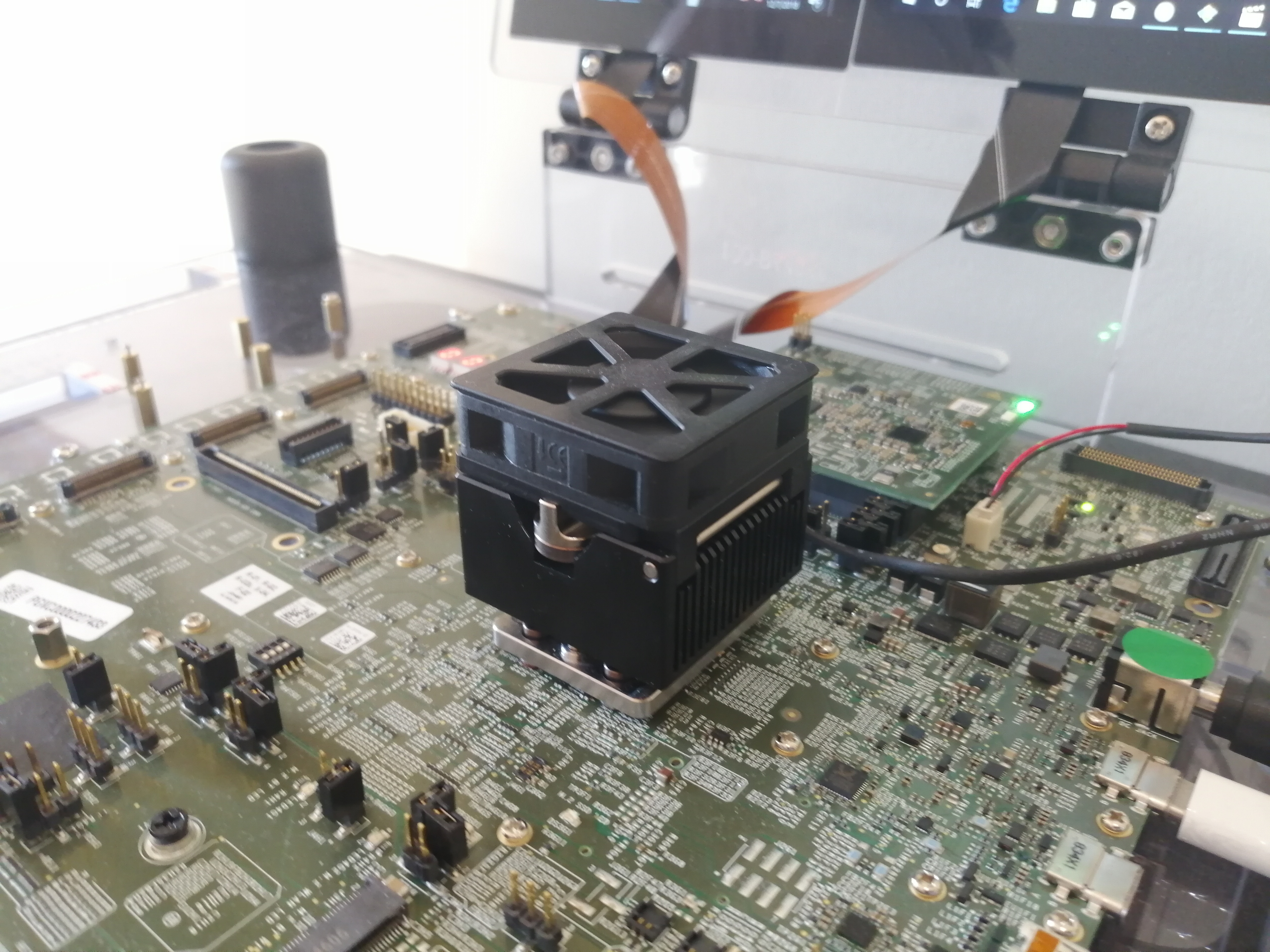
The demo system that Intel had on display looked similar to the previous Sunny Cove design, however this heatsink was smaller and it had a few different connectors. We were told that this chip will support PCIe for M.2 as well as UFS, both of which are found in mobile. There also looked like a couple of SIM card connectors on this motherboard.
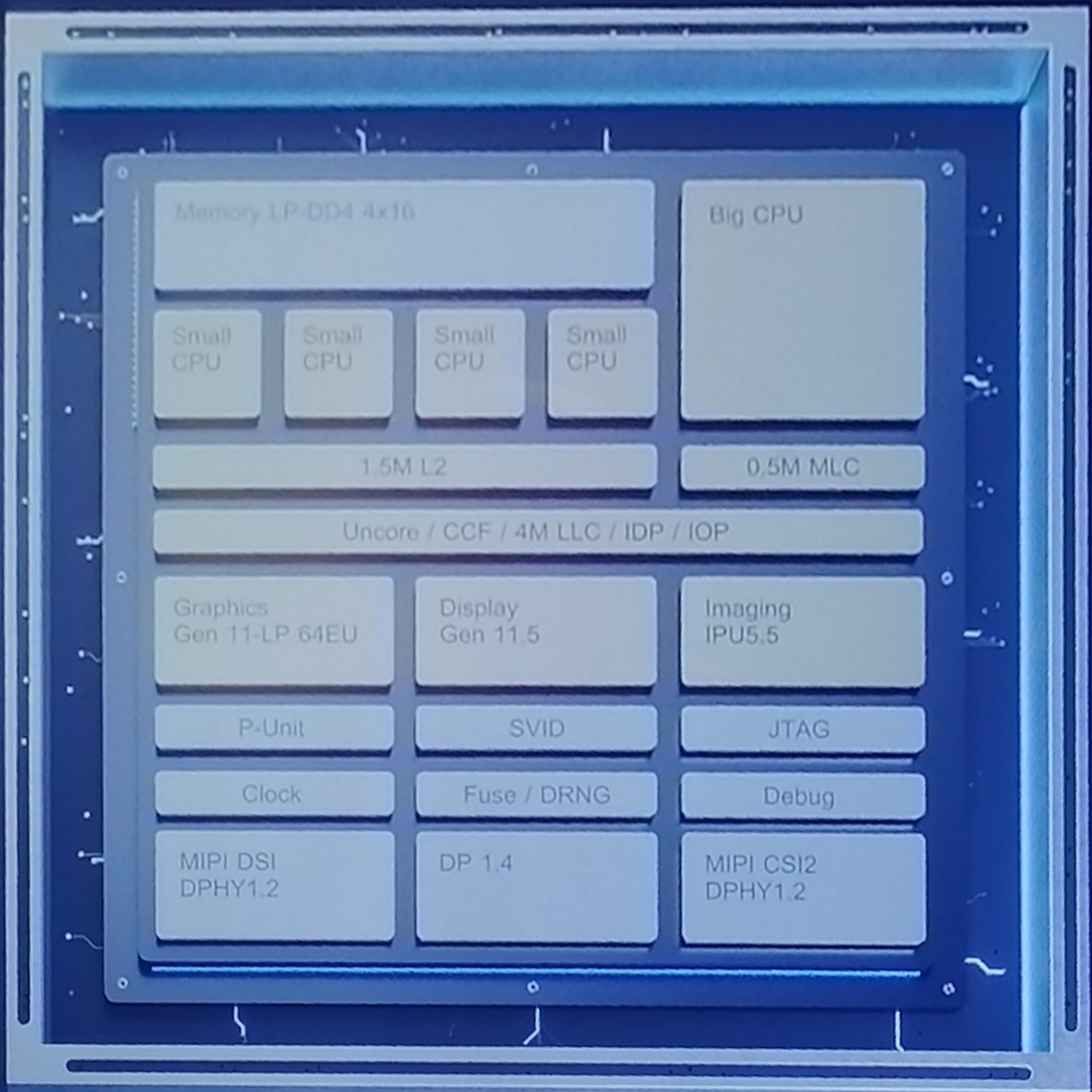
The key part of this discussion however is this block diagram that was on one of the Intel slides. Here we see a single ‘Big CPU’ with 0.5 MB of private medium level cache, four ‘Small CPU’s with a shared 1.5 MB L2 cache, an uncore that has 4MB of last level cache, a quad-channel memory controller (4x16-bit) with support for LPDDR4, a 64 EU design with Gen11 graphics, the Gen 11.5 display controller, a new IPU, MIPI support with DisplayPort 1.4, and all of this in a tiny package. Seriously though, this has the potential to be a large revenue stream for Intel. They’ve made this chip, which allows the cores to enter C6 sleep states when not in use, that has a die size smaller than 12x12mm (144 mm2), and target the sub-7W fanless device market. That’s with a big Core, four Atom cores, and a GT2 64 EU design.
Intel actually says that the reason why this product came about is because a customer asked for a product of about this performance but with a 2 mW standby power state. In order to do this, Intel created and enhanced a number of technologies inside the company. The final product is apparently ideal for the customer, however the chip will also be made available for other OEMs. In our Q&A session with the senior members of Intel, it was clear that this technology is still in its infancy, and Intel now has a new toy to play with. Jim Keller stated that internally they are trying lots of new things with this technology to see what works and what would make a good product, so we should be seeing more Foveros designs through 2019 and 2020. One of the more sedate talks at the event was discussing Intel’s approach in the datacenter. We’ve covered this story in detail, especially at Intel’s Data-Centric Summit only a few months ago. Intel has stated that Cascade Lake and Cooper Lake are the next two products for the enterprise market, both built on 14nm, focusing on enhanced security as well as AI instructions to help with acceleration. We also know that after these two Intel will have Ice Lake Scalable built on 10nm, but that’s about it.
To be honest, we don’t actually know much more than what we did back then. Intel confirmed that Ice Lake will be built using Sunny Cove cores. But Intel also showed off what they said was an Ice Lake Xeon 10nm processor and package, as shown in the image above. Color me skeptical, but what was held up is likely either not ICL-SP or just silicon that doesn’t work. In order to make those products, Intel would have to have pumped out at least one large (350mm2+?) die that worked and then put it into a package with a heatspreader. Intel finally seems to be happy discussing a few products on 10nm, as shown at this event, but all the 10nm hardware is based on tiny 100mm2 or smaller silicon. Given Intel’s documented problems, I would have loved that CPU that was held up in the air to be Ice Lake-SP. But I’ll need to see something more concrete to believe it at this point; it’s too much of a jump. Ending Intel’s Architecture DayAs I’m writing this, it is 3am PT and only a couple of hours away from Intel’s listed embargo time. The event finished 10 hours ago (a few of us skipped the end event drinks to get to writing) and despite the short time to write it all up, it was a good event overall. For the first time in a good while, Intel decided to talk shop, and in an honest way with very little hand waving. One could argue that in every discussion point, Intel raised more questions than they answered, but the positive here is that questions are being answered, and Intel is willing to share things like roadmaps into 2021, demonstrations of some exciting new products for 2019/2020, and a taste of how they are progressing in both manufacturing and microarchitecture. Hopefully Intel will feel the same and this can become a yearly cadence. The trio of Keller, Koduri, and Murthy, is a strong team to field to the press, and this event fits that bill. To end this piece, I’m going to put in the Q&A section from day’s presentations, as well as some of the questions put in my particular round-table. It’s an interesting read, and it helps that Jim is full of memorable quotes. Q&A with Raja, Jim, and MurthyThrough Intel’s Architecture Day, the company did a couple of side discussions for a few journalists to speak to Raja Koduri and Jim Keller in a round-table format. Beyond that, Murthy Renduchintala and Raja also held a Q&A session at the end of the day. They answered questions on 10nm, the new Foveros technology, Thunderbolt 3 adoption, and how Intel will approach 5G. For this article, the Questions and Answers will be listed as an abridged version of the responses, due to time constraints and live transcription, with questions grouped based on topic. Different members of the press asked these questions.
Q: A lot of the CPU microarchitecture at Intel has been hamstrung by delays on process node technology. What went wrong, and what steps have been made to make sure it doesn't happen again? R/J: Our products will be decoupled from our transistor capability. We have incredible IP at Intel, but it was all sitting in the 10nm process node. If we had had it on 14nm then we would have better performance on 14nm. We have a new method inside the company to decouple IP from the process technology. You must remember that customers buy the product, not a transistor family. It’s the same transformation AMD had to go through to change the design methodology when they were struggling. At Apple it was called the ‘bus’ method. M: This is a function of how we as a company used to think about process node technologies. It was a frame tick (limiting factor) for how the company moved forward. We've learned a lot about how this worked with 14nm. We now have to make sure that our IP is not node-locked. The ability to have portability of IP across multiple nodes is great for contingency planning. We will continue to take aggressive risks in our designs, but we also will have contingency. We need to have as much of a seamless roadmap as possible in case those contingencies are needed, and need to make sure they are executed on ASAP if needed to keep the customer expectations in line. You will see future node technologies, such as 10/7, have much more overlap than before to keep the designs fluid. Our product portfolio on 14nm could have been much better if our product designs were not node-locked to 10nm. R: In the future there will be no transistor left behind, no customer left behind, and no IP left behind. Q: Will we ever see a 10nm monolithic desktop CPU at the high end? R: Yes. Q: How is 10nm? Has it changed? R: It is changing, but it hasn't changed. There are a lot of lessons learned in how Intel approached it to begin with. We are established a much better model between manufacturing and design. We want good abstractions in product and process node going forward. When everything was going well, this issue didn't manifest and so wasn't an issue. There's complexity here when something bad happens on process, so the whole pipeline clogs up - the rest of the world solves this with abstraction. We need to make sure it won't happen again, and we have a desire to build resilience in the roadmap.
Q: Are there plans for mixed SoCs, combining CPU / GPU / AI / FPGA ? R: In our roadmap there will be scalable vector/matrix combinations. What our customers want are very scalable solutions. Customers want similar programming models regardless of the silicon. Q: What has been the effect of hiring Raja/Jim and bringing outsiders to Intel? M: Intel is very innovative. We want to add to that chemistry and make sure we bring in people who understand Intel but also bring in good ideas. It's about respecting the rest of the market and make sure Intel is competitive. It's balancing the centre of internal debates by making sure we are challenging internal beliefs and the status quo by bringing in people who have done this sort of thing before. It shows to Intel's strengths in its ability to absorb interesting ideas from the outside. We went for the very best on the outside because that was what required to join with the very best on inside.
Q: What is Intel’s current approach to 5G, given the topics discussed today? M: We think about 5G from the datacentre to the network to the edge and to the device. We at Intel believe the transition to 5G and its implications on the network, in terms of accelerating data and catalysing a software defined network where bespoke silicon gets replaced by containers, is as transformative as the jump from analogue to digital. It will accelerate the ‘cloudification’ of the network. The edge is important, especially to minimize latency for new services. Sub-millisecond latency for these services is critical. The over-the-air interface is important too. The intelligent cloud domain is going to be the flywheel about how fast the industry evolves. We mentioned in November that our XMM 5G modem will be in the hands of partners in the second half of 2019 with products in early 2020. It is a multi-mode 5G LTE architecture from day one, supporting all 3 mmWave bands, and sub-6 GHz frequencies. Q: As Thunderbolt 3 requires additional chips, how do you see future OEM adoption? M: Integrated Type-C Thunderbolt 3 is the first generation. We will refine it in the future - that's the natural genealogy of the technology. We constantly think about how much we integrate into the chip and how much we leave on the board. R: This is a big IP challenge, not only for TB3, but for other IP. Integrated PHYs are important. For example, by disaggregating the transceiver in our FPGA line-up, it has allowed us to focus on that decoupled IP a lot.
Q: In the demo of FOVEROS, the chip combined both big x86 cores built on the Core microarchitecture and the small x86 cores built on the Atom microarchitecture. Can we look forward to a future where the big and little cores have the same ISA? R: We are working on that. Do they have to have the same ISA? Ronak and the team are looking at that. However I think our goal here is to keep the software as simple as possible for developers and customers. It's a challenge that our architects have taken up to ensure products like this enter the market smoothly. We’ll also have a packaging discussion next year on products like this. The chip you see today, while it was designed primarily for a particular customer to begin with, it’s not a custom product, and in that sense will be available to other OEMs. M: We've made the first step on a journey. That first step is a leap, and the next step is incremental. As we've said about One API strategy – if we homogenise the API then it'll go into all our CPUs. FOVEROS is also a new part/product that shows that we had a gap in our portfolio – it has helped us create technologies to solve an issue and we expect to expand on this in the future with new IP. Q: Are you having fun with FOVEROS? J: Because Raja deals in GPUs, he’s having fun with high bandwidth communications between compute elements. It's a new technology and we're having some experimentation with it. What is frustrating is that as an industry we hit a limit for current flux density a year before stacking technology became viable, so for high performance on stacking we're trying a lot of things in different areas. There's no point having to make thermal setbacks if it also removes the reason why you're using the technology. But we're having fun and trying a lot, and we'll see FOVEROS in a number of parts over the next 5 years. We will find new solutions to problems we don't even know exist yet.
Q: When is Manufacturing Tech Day? M: We will tell you when it happens! I'm sure you all have opinions on Intel 10nm right now and yes we are looking at what we're doing, eating an amount of humble pie, but we're re-adjusting our process to make sure that we can take the best process no matter what the product is. The title of this page was a quote from Jim during the Q&A: 'At some point in the future you'll read an article with the title Intel Made Something Really Funny.'. I think I win this bet... | |||||||||||||||||||||||||||||||||||||||||||||||||||||||||||||||||||||||||||||||||||||||||||||||||||||||||||||||||||||||||||||||||||||||||||||||||||||||||||||||||||||||||||||||||||||
| Posted: 12 Dec 2018 03:00 AM PST If you’ve spent any time looking at DIY smart home security products, you’ll have come across Ring and Nest. These aren’t the only companies in this space, but they are two of the biggest names, and each is fighting hard to win your business. Many articles compare the features, specifications, pluses and minuses of specific Nest and Ring products—including the in-depth reviews here on TechHive—but choosing one is about much more than the gadget you’re buying. Your choice can affect a lot of the other technology in your smart home, so you need to consider the big picture. Google vs. AmazonYou’ll find wo of the biggest tech companies on the planet behind this competition: Google acquired Nest in 2014 for $3.2 billion, while Amazon bought Ring in 2018 for reportedly more than $1 billion.  Martyn Williams/IDG Martyn Williams/IDG Ring jumpstarted the video doorbell industry. They didn’t make these investments just to help you see who’s at the front door. Each company wants to dominate your home, and these products—along with the Google Home and Amazon Echo smart speakers—play a big part. Google wants to know more about your life so it can serve you ads, while Amazon wants to sell you stuff directly. Two companies, two ecosystemsIt’s not surprising that the competition has not brought compatibility. Nest products all tightly tie into the Google Home app and can be commanded by Google Assistant. With Ring products, you get great compatibility with Amazon Echo speakers and tight integration with Alexa. Incorporate either family of products into the non-preferred ecosystem and you’ll encounter limited functionality. You can pair a Nest Learning Thermostat with Alexa, for example, and control your HVAC system with voice commands. Do the same with a Nest Cam and you can ask Alexa to display a real-time video feed on your Amazon Echo Show. But you can’t ask Alexa to arm your Nest Secure home security system.  Google Google Nest products are more compatible with Google Home smart speakers, including the display-equipped Google Home Hub shown here. Use a Ring security cameras with a Google Home smart speaker, and you’ll get an even more limited feature set: You won’t be able to stream video from any of Ring’s cameras to a Google Home Hub, for instance, or to a TV with a Google Chromecast plugged into it. If you’ve already invested in other smart home gadgets, and are now shopping for a smart speaker or a more comprehensive system that can incorporate what you already have, that compatibility—or the lack thereof—should be a major factor in your decision. Currently, you’ll discover that a much larger number of products interact with Amazon Alexa than with Google Assistant, mainly because Amazon was faster to offer its technology to other companies. Google, however, is catching up rapidly.  Samsung Samsung Nest and Ring aren't the only smart home games in town. Samsung's SmartThings is another powerful contender. This is also a great time to consider other home ecosystems. Google and Amazon aren’t the only games in town. If your primary concern is home security, Nest and Ring are both great choices. But if you’re more interested in wireless control of your home’s lighting, and an outdoor camera or video doorbell is only an add-on, you might be better looking at something like Samsung SmartThings as the basis for your network. Features and functionsOne of the biggest differences between Nest and Ring is the way in which video is streamed and stored from each company's cameras and video doorbells and how much you'll pay for that capability. Nest cameras stream video continuously and store everything for the length of your Nest Aware subscription (more on pricing below). That can be an advantage because you have a record of everything that happened within view of the camera, whether the motion detector was triggered or not. And Nest offers some great tools for scrubbing that footage to find the specific events you're looking for. If you don't subscribe to Nest Aware, however, Nest cameras will stream video only while you're watching the live stream on a smartphone, tablet, or computer.  Nest Labs Nest Labs Nest Labs has more sophisticated security cameras than Ring, but they're considerably more expensive--especially when you take subscriptions into account. Ring also requires a subscription if you want its cameras to record and upload video, but it does so only when it detects motion. The advantage here is that Ring puts much less demand on your home internet connection. A Nest Cam on a Nest Aware subscription will eat up tens to hundreds of gigabytes of data per month, so watch out if your ISP imposes a data cap. You'll also want to be aware of how fast the upload side of your broadband connection is. Most ISPs emphasize only their download speeds, because they assume consumers are focused on consuming content over the internet (streaming video, for instance). And most consumer broadband services are asynchronous, meaning upload and download speeds are different (with upload speeds nearly always being a fraction of download speeds). Ring suggests you have a minimum upload speed of 2Mbps for its 720p streams, while Nest's recommendation varies from 0.8Mbps for a low-resolution stream (720p) to 4Mbps for a high-definition (1080p) stream. System expansion optionsNest makes its own thermostat and smoke/carbon-monoxide alarm that can be used separately or integrated into its Nest Secure system. Ring has certified a combo smoke/CO detector from First Alert for use with its Ring Alarm security system. Ring has also announced, but is not yet shipping, a smoke/CO "listener" that will send an alert when your existing smoke and carbon-monoxide detectors go off, and a flood and freeze sensor that will alert you to the presence of water where it shouldn't be, as well as freezing temperatures that could lead to a burst pipe.  Nest Labs Nest Labs Nest Labs is ahead of the game when it comes to integrating smart locks into its home security system. Nest Secure does not currently support smart lighting directly, so you can't program it to turn on a smart bulb when a motion or door/window sensor is tripped, but you can link the motion sensor in a Nest Nest Cam to do this with smart lighting products from Philips Hue, LIFX, and Lutron Caseta. The hub in the Ring Alarm system is equipped with ZigBee and Z-Wave radios, but those components are currently dormant. There is no way to integrate smart lighting into a Ring Alarm system today. You can integrate the Nest x Yale smart lock into a Nest Secure system, so that when you unlock the door using its keypad, it will automatically disarm the security system. The Ring app is compatible with smart locks from Kevo, Kisi, Lockitron, and LockState, but this functionality doesn't currently extend to disarming a Ring Alarm system. PricingThe price gap between Ring and Nest is pretty narrow when you’re looking at a single product, but it grows as your system expands. Subscription services are optional in both ecosystems, but in both cases, these products are much less appealing without them.  Ring Ring Be sure you take the price of each company's not-really-optional subscription plan into account before you make an ecosystem decision. Ring charges $3 per month to store video from its doorbell or home security cameras in the cloud, while Nest charges $5 per month for its Nest Aware service. Not a big difference, right? With Ring, that fee goes up to $6 per month for two cameras and $9 for three, but then something good happens. For $10 per month you get support for an unlimited number of cameras, plus professional monitoring for a Ring Alarm system if you own one, with no long-term commitment. Professional monitoring is when a company monitors your alarm and will call you—and the police if necessary—when the alarm is triggered. Nest Aware jumps from $5 for the first camera to an additional $3 for every subsequent camera—there’s no point at which you stop being charged per device. While it's true that you're getting a lot more cloud storage with Nest Aware (because video is streaming 24/7), you need to be aware that professional monitoring with a Nest Secure system is a wholly separate and not unsubstantial subscription: $19 per month if you commit to a three-year contract, or $29 per month for a month-to-month contract you can exit at any time. Without considering the prices for the starter kits and the rest of the components you might want, a professionally monitored Ring Alarm security system with one video doorbell and three cameras will cost you $10 per month. A similarly configured Nest Secure system will cost either $33 or $43 per month, so consider your expansion plans because these "optional" subscriptions really aren't. The bottom lineTake your time, think about how you might expand your home security system, and consider which digital assistant you'll want to use to interact with it. Thorough consideration at the earliest stages of your planning will have a huge impact on how satisfied you are and how much money you'll spend on it, now and in the future. | |||||||||||||||||||||||||||||||||||||||||||||||||||||||||||||||||||||||||||||||||||||||||||||||||||||||||||||||||||||||||||||||||||||||||||||||||||||||||||||||||||||||||||||||||||||


| You are subscribed to email updates from Technology - Latest - Google News. To stop receiving these emails, you may unsubscribe now. | Email delivery powered by Google |
| Google, 1600 Amphitheatre Parkway, Mountain View, CA 94043, United States | |
This post have 0 komentar
EmoticonEmoticon